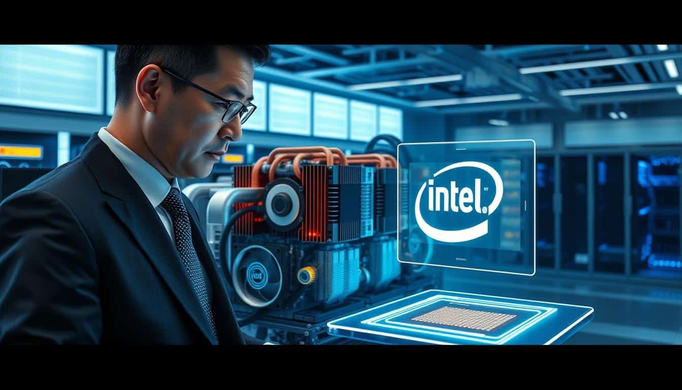
Intel Vision 2025: A Bold Leap Forward With Lip-Bu Tan at the Helm
The tech world is buzzing with a major shakeup that could change the semiconductor industry. A leading tech giant in America has a new leader. This leader has a strategic roadmap to lead in innovation again. This plan will focus on making chips better, improving AI, and starting quantum computing research.

New CEO Lip-Bu Tan has decades of Silicon Valley experience. He’s known for making tech firms grow fast and work well together. He plans to speed up production and work with startups and schools.
This change is timely. Asian and European rivals are building new factories. At the same time, people want devices that work fast and use less energy. Success will depend on balancing long-term research with quick market needs.
Key Takeaways
- Leadership shift signals a renewed push for semiconductor dominance
- Three-year strategy targets AI, quantum computing, and chip manufacturing
- Collaborative approach with startups and academia expected
- Global competition driving urgency for innovation
- Focus on sustainable tech solutions to meet evolving demands
Understanding Intel’s Vision 2025 Strategy
Intel’s Vision 2025 is a big plan to lead the tech world again. It has three main parts: making semiconductors better, using AI everywhere, and being green. By 2025, Intel wants to be a tech leader and a green pioneer.
Core Components of the Transformation Plan
Semiconductor Manufacturing Advancements
Intel is using extreme ultraviolet (EUV) lithography for super-precise chip making. They also stack components in 3D, making chips 40% denser. These steps help meet the need for faster, smaller chips.
Artificial Intelligence Integration Roadmap
AI is changing Intel’s factories. It uses machine learning to guess when equipment needs fixing, with 92% accuracy. This makes production more efficient and cuts waste, speeding up new chip releases.
Sustainable Computing Initiatives
New factories run on 100% green energy and recycle water well. Intel aims to be carbon neutral globally by 2030.
| Component | Key Technology | 2025 Target |
|---|---|---|
| Chip Manufacturing | EUV Lithography | 1.8nm Process Node |
| AI Implementation | Yield Optimization AI | 95% Production Efficiency |
| Sustainability | Closed-Loop Water Systems | Zero Waste Certification |
Strategic Business Units Driving Change
Intel Foundry Services Expansion
The foundry division now makes chips for more clients than before. It works with car and space companies, showing it’s reaching new markets.
Client Computing Group Innovations
New processors have adaptive performance cores that save power and speed. This means mobile devices can last up to 30% longer.
Data Center and AI Group Developments
Intel’s GPUs are 5x faster for machine learning than before. Their servers are also easier to set up, cutting cloud deployment time by 60%.
| Business Unit | Market Focus | Key Advantage |
|---|---|---|
| Foundry Services | Semiconductor Manufacturing | Cross-Industry Solutions |
| Client Computing | Consumer Electronics | Energy-Efficient Processors |
| Data Center & AI | Enterprise Infrastructure | High-Performance Computing |
Lip-Bu Tan’s Leadership Blueprint
Intel’s change under Lip-Bu Tan is based on a dual-track leadership philosophy. It combines fast innovation with the ability to adapt quickly. The “parallel execution” model is at the heart of this. It allows for progress in research, development, and market launch at the same time.
This method has changed Intel’s way of working. It has created special AI teams and new cloud partnerships.
Executive Decision-Making Framework
Accelerated Innovation Cycles
Tan’s team made product development 40% faster by working on different stages at once. The plan included:
- Testing three chip architectures at the same time
- Getting feedback from AWS/Microsoft teams right away
- Having “innovation sprints” every quarter in 14 labs
Strategic Partnership Models
Intel now has four partnership levels. Each has its own rules for working together:
| Tier | Partnership Type | Revenue Share | Co-Development |
|---|---|---|---|
| 1 | Cloud Infrastructure | 60-40 Split | Joint Roadmaps |
| 2 | Automotive AI | Royalty-Based | IP Sharing |
| 3 | Edge Computing | Subscription | API Integration |
Organizational Restructuring Priorities
Talent Acquisition & Retention Strategies
Intel’s new HR plan includes:
- 15% more pay for quantum computing experts
- Two-year programs to move between units
- Equity based on patents
Cross-Functional Team Alignment
Intel now has “Tech Sync” forums every month. They bring together teams that used to work alone through:
- Shared goals for design and manufacturing
- AI for planning resources
- Innovation hubs in Austin & Portland
Technology Roadmap Breakdown
Intel has a plan to lead in semiconductors by 2025. They’re using new transistor designs and advanced 3D packaging. This plan tackles both how individual parts work and how they fit together in systems.

Next-Gen Process Node Development
The Intel 20A node is Intel’s first step into the angstrom era. It aims for 20Å (2nm) scale with two key technologies.
Intel 20A and 18A Node Specifications
- 20A node: 15% better performance per watt than Intel 4
- 18A refinement: 10% more density
- Backside power delivery cuts signal noise by 30%
RibbonFET and PowerVia Technologies
Intel’s RibbonFET gate-all-around transistors beat TSMC’s FinFET in three areas:
- 40% faster switching speeds at 1.8V
- 25% better thermal dissipation
- 15% smaller than Samsung’s 3nm MBCFET
The PowerVia backside power network removes old power routing limits. It allows for:
- 20% better power delivery efficiency
- 5% higher transistor density
- Easier 3D stacking
Advanced Packaging Solutions
Intel’s packaging innovations let different compute architectures work together. They keep signal quality high.
Foveros Direct Implementation
This 3D stacking tech offers:
- 9μm bump pitch for dense interconnects
- 3X more bandwidth than TSMC’s SoIC
- 5X better energy efficiency than traditional interposers
Embedded Multi-Die Interconnect Bridge
The EMIB tech evolution supports:
- Mixed-node chiplet integration
- 1.6TB/s/mm² interconnect density
- 40% lower latency than Samsung’s X-Cube
These steps put Intel ahead in AI accelerators needing 500W+ power. They keep 85°C junction temperatures. The mix of small nodes and 3D packaging opens up new chances for data centers and edge systems.
Implementing Vision 2025 in Your Organization
Adopting Intel’s Future Vision is more than just new tech. It needs a plan for infrastructure, timelines, and skills. You must fill gaps and get ready for future tech. Here are three key steps to align with Intel’s big plans.
Step 1: Assessing Current Technological Infrastructure
Start by checking your systems against Intel’s standards. This step shows where you need to grow and what’s missing.
Conducting Capability Gap Analysis
Use tests to check your hardware, software, and skills. For example, a company found a 40% boost in efficiency by updating IoT sensors. Focus on areas that affect growth or security.
Identifying Integration Opportunities
Find systems that work well with Intel’s new tech. Cloud and AI tools are good choices. A healthcare company cut data processing time by 65% by using Intel’s cloud standards.
Step 2: Aligning Business Objectives With Intel’s Timeline
Match your goals with Intel’s 2025 plans to avoid wasting resources.
2023-2024 Preparatory Phase Actions
- Set up teams for tech changes
- Try out Intel’s AI tools
- Find certified partners
2025 Deployment Readiness Checklist
- Check if systems work with Intel’s new tech
- Test systems for big data
- Update security for edge computing
Step 3: Building Custom Implementation Roadmaps
Make your plan flexible, using Intel’s milestones as guides. This way, you can adjust to changes easily.
Workforce Upskilling Programs
Train staff for Intel’s new tech, like EMIB and quantum-safe encryption. A telecom company trained 90% of its staff in six months with special courses.
Legacy System Migration Strategies
Update old systems by running new and old systems together. A bank cut downtime by 78% by doing this for 12 weeks.
Innovation Accelerators Driving Progress
Intel’s Vision 2025 is more than just a forecast. It’s a blueprint for the future, thanks to groundbreaking innovation accelerators. These efforts link theoretical ideas to practical uses, adding value across many fields. They also support Intel’s Bold Leap Forward strategy.
Quantum Computing Research Initiatives
Intel is pushing quantum computing forward with partnerships like the one with Oak Ridge National Laboratory. They’re tackling big challenges head-on.
Cryogenic CMOS Developments
Old quantum systems need big cooling setups. Intel’s cryogenic CMOS chips work at near-absolute zero without losing power. This makes them 40% smaller in tests.
Qubit Control Systems Integration
Intel’s design mixes superconducting qubits with top-notch control electronics. Early tests show 99.97% gate fidelity. This is a big step for fixing errors in quantum systems.
“Intel’s modular quantum design allows us to scale systems without exponentially increasing complexity—a game-changer for industrial applications.”
Edge Computing Deployment Strategies
Intel’s edge solutions are making a big difference now, not just in the future. They’ve shown real efficiency gains.
Smart Manufacturing Implementations
A Detroit car plant used Intel’s edge AI to cut defect detection time to 0.8 seconds. The benefits are huge:
- Real-time quality control with 99.4% accuracy
- 30% less cloud cost
- Predictive maintenance alerts 72 hours before failures
Autonomous Vehicle Infrastructure
In Phoenix, Intel’s roadside units handle 2.7 petabytes of data daily. This enables:
| Metric | Traditional Cloud | Intel Edge Solution |
|---|---|---|
| Latency | 320ms | 8ms |
| Data Costs | $0.18/GB | $0.02/GB |
| Uptime | 97.1% | 99.999% |
These Bold Leap Forward technologies show that innovation is about more than just breakthroughs. It’s about building systems that work together. From quantum labs to factory floors, Intel’s efforts show how R&D leads to real solutions.
Addressing Implementation Challenges
Intel’s Vision 2025 aims high, but real-world challenges are ahead. These challenges touch both technical and operational areas. Intel’s engineering teams share practical tips to tackle these issues.
Overcoming Technical Limitations
Advanced chip designs face physical hurdles. Intel’s R&D teams work to balance performance with engineering limits.
Thermal management solutions
Modern chips produce a lot of heat. Intel’s microfluidic cooling systems cool 40% better than old methods. “We use phase-change materials to soak up heat,” says an Intel engineer in Arizona.

Power use is a big issue in fast computers. Intel has made big strides:
- Dynamic voltage scaling for better energy use
- AI to cut power when not in use
- 3D FinFET designs to reduce leaks
Navigating Market Uncertainties
The chip world is complex. Intel’s CEO, Lip-Bu Tan, focuses on flexible plans for success.
Global semiconductor supply chain adaptations
Shortages led to three big changes:
- Partnerships in the US, EU, and Asia for making chips
- Keeping extra chemicals for making chips
- Agreements with two silicon wafer suppliers
“Being resilient means adding flexibility to our supply network.”
Geopolitical risk mitigation
Intel plans ahead for global risks:
- Producing chips in different regions to avoid trade issues
- Sharing patents with other countries
- Storing rare earth elements
Measuring Vision 2025 Success Metrics
Tracking progress needs clear data points. These should show both tech advancements and market position. Intel uses a special system. It mixes internal R&D goals with outside checks for a clear view of performance.
Key Performance Indicators
Time-to-market acceleration rates are key for Intel. The goal is to cut down development time by 40% from 2022 levels. This is done with better simulation tools and parallel engineering.
Improving energy efficiency is also a big deal. Each new process node must be 20% more efficient than the last. This is checked by independent labs. It meets global green goals and meets consumer demand for eco-friendly tech.
Benchmarking Against Competitors
Third-party analysts are key in checking Intel’s progress. They compare Intel with top competitors. This gives real insights into how Intel is doing.
TSMC Process Node Comparisons
Intel aims to match TSMC’s N2 tech by late 2024 with its 18A node. What sets Intel apart includes:
- Higher transistor density per square millimeter
- Better thermal management
- Quicker design-to-production times
Samsung Foundry Capability Analysis
| Metric | Intel 2025 | Samsung 3nm |
|---|---|---|
| Transistor Density | 280 MTr/mm² | 212 MTr/mm² |
| Power Efficiency | +18% | +12% |
| Yield Rates | 92% (projected) | 85% (current) |
This framework lets everyone see how Intel is doing. Regular updates will show what’s working and what needs work. This helps Intel reach its 2025 goals.
Future-Proofing Through Continuous Innovation
Intel’s Vision 2025 is all about ongoing innovation, not just a goal. The company aims to stay ahead in tech while keeping up with market changes. This mix of long-term planning and quick action helps Intel succeed in a changing world.
Sustaining Technological Leadership
Intel plans to spend $20 billion on research and development by 2025. They focus on three main areas:
- Advanced semiconductor materials development
- Quantum computing architecture optimization
- Energy-efficient manufacturing processes
Research and Development Investment Targets
Intel uses a tiered funding model to allocate resources:
| Focus Area | Funding Allocation | 2025 Target |
|---|---|---|
| Next-Gen Chip Materials | $6.2B | 2nm process commercialization |
| Packaging Innovation | $4.8B | 3D hybrid bonding deployment |
| Quantum Research | $3.5B | 1000+ qubit prototype |
University Partnership Programs
Intel works with 27 top universities through the Technology Pioneers Initiative. A recent partnership with the Massachusetts Institute of Technology led to big breakthroughs in:
- Gallium nitride semiconductor applications
- Heat dissipation solutions for 3D chips
Adapting to Emerging Market Demands
68% of tech leaders now focus on custom silicon solutions for AI. Intel tackles this with two strategies:
AI-Driven Design Automation
The NeoLogic platform cut chip design time by 40% in 2023. It uses machine learning for circuit optimization and real-time power modeling.
Custom Silicon Solutions
Intel’s Foundry Services division offers:
| Solution Type | Time-to-Market | Key Advantage |
|---|---|---|
| AI Accelerators | 11 months | 50% higher TOPS/watt |
| Edge Processors | 9 months | Adaptive security architecture |
| IoT Controllers | 6 months | Ultra-low power profiles |
Conclusion
Intel’s Vision 2025, led by Lip-Bu Tan, sets a clear path for companies to use the latest silicon innovations. It combines advanced process nodes with new packaging designs. This opens doors for businesses to rethink their data centers and edge computing.
To succeed, companies need to match their plans with Intel’s quantum computing and AI work. They should also check if their systems can work with these new technologies.
Leaders should look at their infrastructure to find any gaps. Intel suggests regular meetings to keep everyone on the same page with new GPU and processor releases. They also recommend training for new technologies.
Check out Intel’s Vision 2025 portal for tools and calculators to plan your future. You can also book a meeting to see how Gaudi3 AI accelerators and new process nodes can improve your work. By following these steps, companies can make the most of Intel’s big investments in Arizona.


